Showing posts with label dc. Show all posts

Wednesday, December 25, 2013

DC or AC Voltage Indicator

Detects 1.8 to 230 Volts DC or AC, Minimum parts counting

This circuit is not a novelty, but it proved so useful, simple and cheap that it is worth building. When the positive (Red) probe is connected to a DC positive voltage and the Black probe to the negative, the Red LED will illuminate. Reversing polarities the Green LED will illuminate. Connecting the probes to an AC source both LEDs will go on.

The bulb limits the LEDs current to 40mA @ 220V AC and its filament starts illuminating from about 30V, shining more brightly as voltage increases. Therefore, due to the bulb filament behavior, any voltage in the 1.8 to 230V range can be detected without changing component values.

Circuit diagram:


DC or AC Voltage Indicator Circuit Diagram

Parts:

P1 = Red Probe
P2 = Black Probe
D1 = 5 or 3mm. Red LED
D2 = 5 or 3mm. Green LED
LP = 1220V 6W Filament Lamp Bulb

Note:
  • A two colors LED (Red and Green) can be used in place of D1 & D2.
Source: Red Free Circuit Design
Read More..

Monday, December 23, 2013

Simple Ac To Dc Converter Circuit Diagram

This is simple Ac To Dc converter circuit diagram. By coupling two back-to-back diodes in series with an ac power circuit, a voltage of about 1.4 Vpp can be obtained. This voltage is useful for exciting the primary coil of a small transformer. The voltage induced in the secondary coil can then be rectified and used to power solid-state control circuits. The forward-voltage drop of the diodes is inherently constant and stable over a wide range of ac-circuit power variations. 

The resulting voltage developed across the transformer windings is also free from variation that might be caused by changes in the circuit`s current or voltage. In the circuit, a lamp (LMP-1) is connected to the primary ac input line (Ll and L2) through a pair of inverse-parallel-connected power diodes (Dl and D2). As power flows to the lamp, a drop of about 0.7 V is alternatively developed across each of the diodes. 

This voltage feeds the primary of a small transformer (Tl). T1 can be a small 8- to 500- transistor radio output, etc. This will deliver about 11 Vpp across its secondary winding. LMP1 can be a small 120-V lamp of 5 to 25 W, etc.

Ac To Dc Converter Circuit Diagram

Ac To Dc Converter Circuit Diagram


Simple Ac To Dc Converter Circuit Diagram
Read More..

Wednesday, December 18, 2013

Dual Output dc dc Converter Circuit Diagram

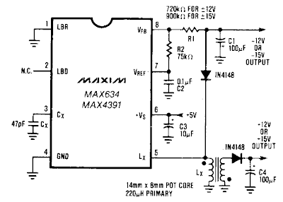
The Dual Output dc-dc Converter Circuit Diagram buck-boost configuration the MAX634 is well suited for dual output dc-dc converters. Only a second winding on the inductor is needed. Typically, this second winding is bifilar-primary and secondary are wound simultaneously using two wires in parallel. 

The inductor core is usually a toroid or a pot core. The negative output voltage is fully regulated by the MAX634. The positive voltage is semi-regulated, and will vary slightly with load changes on either the positive or negative outputs.

Dual Output dc-dc Converter Circuit Diagram

Dual Output dc-dc Converter Circuit Diagram

Read More..

Sunday, September 22, 2013

DC DC Converter From 1 5V To 34V

An interesting DC/DC converter IC is available from Linear Technology. The LT1615 step-up switching voltage regulator can generate an output voltage of up to +34V from a +1.2 to +15V supply, using only a few external components. The tiny 5-pin SOT23 package makes for very compact construction. This IC can for example be used to generate the high voltage needed for an LCD screen, the tuning voltage for a varicap diode and so on. The internal circuit diagram of the LT1615 is shown in Figure 1. It contains a monostable with a pulse time of 400 ns, which determines the off time of the transistor switch.

If the voltage sampled at the feedback input drops below the reference threshold level of 1.23 V, the transistor switches on and the current in the coil starts to increase. This builds up energy in the magnetic field of the coil. When the current through the coil reaches 350 mA, the monostable is triggered and switches the transistor off for the following 400 ns. Since the energy stored in the coil must go somewhere, current continues to flow through the coil, but it decreases linearly. This current charges the output capacitor via the Schottky diode (SS24, 40V/2A). As long as the voltage at FB remains higher than 1.23V, nothing else happens.

DC/DC Converter From +1.5V To +34VAs soon as it drops below this level, however, the whole cycle is repeated. The hysteresis at the FB input is 8mV. The output voltage can be calculated using the formula Vout = 1.23V (R1+R2) / R2 The value of R1 can be selected in the megohm range, since the current into the FB input is only a few tens of nano-amperes. When the supply voltage is switched on, or if the output is short-circuited, the IC enters the power-up mode. As long as the voltage at FB is less than 0.6V, the LT1615 output current is limited to 250mA instead of 350mA, and the monostable time is increased to 1.5µs.

These measures reduce the power dissipation in the coil and diode while the output voltage is rising. In order to minimize the noise voltages produced when the coil is switched, the IC must be properly decoupled by capacitors at the input and output. The series resistance of these capacitors should be as low as possible, so that they can short noise voltages to earth. They should be located as close to the IC as possible, and connected directly to the earth plane. The area of the track at the switch output (SW) should be as small as possible. Connecting a 4.7-µF capacitor across the upper feedback capacitor helps to reduce the level of the output ripple voltage.

DC/DC Converter From +1.5V To +34VThe selection of the coil inductance is described in detail in the LT1615 data sheet at www.linear-tech.com. Normally, a 4.7µH filter choke is satisfactory for output voltages less than 7V. For higher voltages, a 10-µH choke should be used. In the data sheet, the Coilcraft DO1608-472 (4.7 µF) and DO1608-100 (10 µF) are recommended. The Schottky diode must naturally have a reverse blocking voltage that is significantly greater than the value of the output voltage. The types MBR0530 and SS24 are recommended. The shutdown input (/SHDN) can be used to disable the step-up regulator by applying a voltage that is less than +0.25V.

If the voltage at this pin is +0.9 V or higher, the LT1615 is active. You must bear in mind that even when the IC is disabled, the input voltage still can reach the output via the coil and the diode, reduced only by the forward voltage drop of the diode. The second circuit diagram for the LT1615 (Figure 2) shows how you can make a symmetric power supply using this switching regulator. Here the switch output of the IC is tapped off and rectified using a symmetrical rectifier. The voltage divider at the positive output of the rectifier determines the output voltage.
Read More..

Tuesday, September 10, 2013

50W DC DC Converters TRACOPOWER with the Highest Power Density

TRACOPOWER launches the high performance TEN50 Series with 12 models providing 50W power in a 1”x 2”x 0.4 “ compact package. Today already almost all of applications require a high efficiency of a voltage conversion. When we add to this requirement also saving of space and a galvanic isolation, we´ll get to widely used components – DC/DC modules. The TEN 50 Series models feature a very high efficiency of up to 92%. Excellent efficiency is maintained in over a wide load range and no minimum load is required for an accurate output regulation. They are available in three basic groups – TEN 50-12xx, TEN 50-24xx a TEN 50-48xx with a wide input voltage range (2:1).

50W DC/DC Converters TRACOPOWER with the Highest Power Density
 
Low thermal losses and the use of highest grade components allow an operating temperature range of –40°C to +85°C while up to 55°C no forced air cooling is required. With an optional heat-sink this temperature can even be increased. An operation without a forced air cooling is possible even at higher temperatures – at an adequate power derating ( 2%/K above 55°C and 2,5%/K above 65°C). The TEN 50 Series comes with remote On/Off function and have an adjustable output voltage (± 10%). Protection against overload and short-circuit, very compact dimensions and a 1500VDC isolation enable usage of TEN 50 modules in virtually any power application.
Read More..

Friday, April 5, 2013

9V DC Adapter With Battery Backup

With just a low cost DC adapter and the circuit described here it is possible to build a low cost stabilized, uninterruptable 9V supply. On the grounds of safety and economy, a simple unstabilized 12V D.C. adapter is used as the power source, a universal adapter with its output set to 12 V will do equally well. The output voltage of an adapter under low load conditions (up to approximately 1/3 of the rated output current) is over 15 V, even at the rated output current, there will be sufficient voltage to supply a 9 V voltage regulator. The rating of the DC adapter should be chosen according to the output current required at 9V. Common values are 300mA, 500mA and 1A.

The 9V voltage regulator used in this circuit has a built in thermal shutdown mechanism so that if too much current is drawn from the device, it simply turns off as it overheats and will not supply any current until the case temperature returns to normal. If the unit is intended to supply more than say 150-200mA then to prevent thermal shutdown it will be necessary to fit a heatsink to the voltage regulator. The rule of thumb used to calculate the size of heatsink is that you should be able to touch it during operation at maximum load, without burning you finger. When choosing the DC adapter, it is always better to select one with a higher current rating than is needed this will ensure that its output voltage is high enough to be able to also charge the 12V cells.

DC Adapter with Battery Backup Circuit DiagramAs long as mains voltage is on the DC adapter, the voltage across C1 will be higher than the voltage of the cells. Charging current will flow through R1 and D1 to the cells. Current also flows to the voltage regulator and out to the load connected at the output. Diode D2 in this situation will not conduct because the voltage at its cathode is greater than that at its anode When the mains voltage fails or is turned off, diode D2 conducts and current will now flow from the Nickel Cadmium cells to the voltage regulator, thereby automatically keeping the output voltage at 9V. The value of resistor R1 is chosen so that a charging current to the cells is not greater than 1/10th of the cells capacity (if the cells are rated at 1100mAh, the charging current must not exceed 110mA).

From the point of view of cell longevity it is better to reduce this charging current even further (1/20 or 1/50 C). When calculating this resistor, the value of the no-load voltage should be used. This will give the highest charging current. To calculate the charging current using R1 with a value of 180 Ω. The cells measure 13.8 V when fully charged and the no-load output voltage of the DC adapter is 17V. Charging current is given by the formula: (17V – 13.8V – 0.7V) / 180 = 13.9mA. Substituting the actual measured values in this formula will enable you to calculate the value of R1 to give the correct charging current for the cells.
Read More..