Showing posts with label amplifier. Show all posts

Monday, December 23, 2013

Precision Headphone Amplifier

Designs for good-quality headphone amplifiers abound, but this one has a few special features that make it stand out from the crowd. We start with a reasonably conventional input stage in the form of a differential amplifier constructed from dual FET T2/T3. A particular point here is that in the drain of T3, where the amplified signal appears, we do not have a conventional current source or a simple resistor. T1 does indeed form a current source, but the signal is coupled out to the base of T5 not from the drain of T3 but from the source of T1. Notwithstanding the action of the current source this is a low impedance point for AC signals in the differential amplifier.

Precision Headphone Amplifier-Circuit-Diagram
Precision Headphone Amplifier Circuit Diagram

Measurements show that this trick by itself results in a reduction in harmonic distortion to considerably less than –80 dB (much less than 0.01 %) at 1 kHz. T5 is connected as an emitter follower and provides a low impedance drive to the gate of T6: the gate capacitance of HEXFETs is far from negligible. IC1, a volt-age regulator configured as a current sink, is in the load of T6. The quiescent current of 62 mA (determined by R11) is suitable for  an output power of 60 mWeff into an impedance of 32 Ω, a value typical of high-quality headphones, which provides plenty of volume.

Precision Headphone Amplifierw

Using higher-impedance headphones, say of 300 Ω, considerably more than 100 mW can be achieved. The gain is set to a useful 21 dB (a factor of 11) by the negative feedback circuit involving R10 and R8. It is not straightforward to change the gain because of the single-sided supply: this voltage divider also affects the operating point of the amplifier. The advantage is that excellent audio quality can be achieved even using a simple unregulated mains supply.  Given the relatively low power output the power supply is considerably overspecified. Noise and hum thus remain more than 90 dB below the signal (less than 0.003 %), and the supply can also power two amplifiers for stereo operation.

The bandwidth achievable with this design is from 5 Hz to 300 kHz into 300 Ω, with an output voltage of 10 Vpp. The damping factor is greater than 800 between 100 Hz and 10 kHz. A couple of further things to note: some-what better DC stability can be achieved by replacing D1 and D2 by low-current red LEDs (connected with the right polarity!). R12 prevents a click from the discharge of C6 when headphones are plugged in after power is applied. T6 and IC1 dissipate about 1.2 W of power each as heat, and so cooling is needed. For low impedance headphones the current through IC1 should be increased. To deliver 100 mW into 8 Ω, around 160 mA is required, and R11 will need to be 7.8 Ω (use two 15 Ω resistors in parallel).

To keep heat dissipation to a reasonable level, it is recommended to reduce the power supply volt-age to around 18 V (using a transformer with two 6 V secondaries). This also means an adjustment to the operating point of the amplifier: we will need about 9V between the positive end of C6 and ground. R4 should be changed to 100 Ω, and R8 to 680 Ω. The gain will now be approximately 6 (15 dB). The final dot on the ‘i’ is to increase C7 by connecting another 4700 µF electrolytic in parallel with it, since an 8 Ω load will draw higher currents.

Source:   http://www.ecircuitslab.com/2012/02/precision-headphone-amplifier.html
Read More..

Friday, December 20, 2013

10W Audio Amplifier With Bass Boost

High Quality, very simple design, No preamplifier required

This design is based on the 18 Watt Audio Amplifier, and was developed mainly to satisfy the requests of correspondents unable to locate the TLE2141C chip. It uses the widespread NE5532 Dual IC but, obviously, its power output will be comprised in the 9.5 - 11.5W range, as the supply rails cannot exceed ±18V. As amplifiers of this kind are frequently used to drive small loudspeaker cabinets, the bass frequency range is rather sacrificed. Therefore a bass-boost control was inserted in the feedback loop of the amplifier, in order to overcome this problem without quality losses. The bass lift curve can reach a maximum of +16.4dB @ 50Hz. In any case, even when the bass control is rotated fully counterclockwise, the amplifier frequency response shows a gentle raising curve: +0.8dB @ 400Hz, +4.7dB @ 100Hz and +6dB @ 50Hz (referred to 1KHz).

 10W Bass Boost Amplifier Circuit diagram:

10W Audio Amplifier with Bass boost Circuit Diagram
Parts:

P1_________________22K Log.Potentiometer (Dual-gang for stereo)
P2_________________100K Log.Potentiometer (Dual-gang for stereo)
R1_________________820R 1/4W Resistor
R2,R4,R8___________4K7 1/4W Resistors
R3_________________500R 1/2W Trimmer Cermet
R5_________________82K 1/4W Resistor
R6,R7______________47K 1/4W Resistors
R9_________________10R 1/2W Resistor
R10________________R22 4W Resistor (wirewound)
C1,C8______________470nF 63V Polyester Capacitor
C2,C5______________100µF 25V Electrolytic Capacitors
C3,C4______________470µF 25V Electrolytic Capacitors
C6_________________47pF 63V Ceramic or Polystyrene Capacitor
C7_________________10nF 63V Polyester Capacitor
C9_________________100nF 63V Polyester Capacitor
D1_________________1N4148 75V 150mA Diode
IC1_________________NE5532 Low noise Dual Op-amp
Q1_________________BC547B 45V 100mA NPN Transistor
Q2_________________BC557B 45V 100mA PNP Transistor
Q3_________________TIP42A 60V 6A PNP Transistor
Q4_________________TIP41A 60V 6A NPN Transistor
J1__________________RCA audio input socket

Power Supply Circuit diagram:

PSU_For_10W_Audio_Amplifier 
Power supply parts:

R11______________1K5 1/4W Resistor
C10,C11__________4700µF 25V Electrolytic Capacitors
D2_______________100V 4A Diode bridge
D3_______________5mm. Red LED
T1_______________220V Primary, 12 + 12V Secondary 24-30VA Mains transformer
PL1______________Male Mains plug
SW1______________SPST Mains switch

Notes:
  • Can be directly connected to CD players, tuners and tape recorders.
  • Schematic shows left channel only, but C3, C4, IC1 and the power supply are common to both channels.
  • Numbers in parentheses show IC1 right channel pin connections.
  • A log type for P2 will ensure a more linear regulation of bass-boost.
  • Do not exceed 18 + 18V supply.
  • Q3 and Q4 must be mounted on heatsink.
  • D1 must be in thermal contact with Q1.
  • Quiescent current (best measured with an Avo-meter in series with Q3 Emitter) is not critical.
  • Set the volume control to the minimum and R3 to its minimum resistance.
  • Power-on the circuit and adjust R3 to read a current drawing of about 20 to 25mA.
  • Wait about 15 minutes, watch if the current is varying and readjust if necessary.
  • A correct grounding is very important to eliminate hum and ground loops. Connect to the same point the ground sides of J1, P1, C2, C3 &C4. Connect C9 to the output ground.
  • Then connect separately the input and output grounds to the power supply ground.
Technical data:

Output power:
10 Watt RMS into 8 Ohm (1KHz sinewave)
Sensitivity:
115 to 180mV input for 10W output (depending on P2 control position)
Frequency response:
See Comments above
Total harmonic distortion @ 1KHz:
0.1W 0.009% 1W 0.004% 10W 0.005%
Total harmonic distortion @ 100Hz:
0.1W 0.009% 1W 0.007% 10W 0.012%
Total harmonic distortion @ 10KHz:
0.1W 0.056% 1W 0.01% 10W 0.018%
Total harmonic distortion @ 100Hz and full boost:
1W 0.015% 10W 0.03%
Max. bass-boost referred to 1KHz:
400Hz = +5dB; 200Hz = +7.3dB; 100Hz = +12dB; 50Hz = +16.4dB; 30Hz = +13.3dB
Unconditionally stable on capacitive loads

Source :  http://www.ecircuitslab.com/2011/05/10w-audio-amplifier-with-bass-boost.html
Read More..

Wednesday, December 18, 2013

200w Audio Power Amplifier

This audio amplifier circuit delivers up to 200 W of top-class quality for loudspeaker from 4 to 16 ohm. Operating voltage is between 24 and 36 V, max 5 A. The frequency response is from 20 to 20000 Hz.  Please take special care that the transistors and the IC’s have been fixed firmly and solely one or two separated cooling elements with sufficient dimensions for this purpose (thermal resistance < 1K/W).

200W Audio Power Amplifier Circuit Diagram :

200w-amplifier-schematic-Circuit diagram
Doing so it is necessary to mount the transistors and the IC’s insulated (with mica washes and plastic nipple). Please make sure before first operation that the transistors and the IC’s really do not have any electrical connection towards the cooling plate! The transistors have to be placed plane and firmly onto the cooling element! It is of extraordinary importance with this high-power amplifier that there is a considerable heat dissipation. The already mounted cooling element should be situated in a well ventilated case.
The PSU should be sufficiently powerful, power consumption of the amplifier may increase up to 5A. In case of using an unstabilised power supply. It is advisable to place a transformer of max 28V.
The amplifier will the show approx. 120W at a 4-Ohm loudspeaker, for it no-load voltage of the power supply will not be to high. If it is desired to use complete power, it is necessary to place a stabilised power supply with approx. 36V 5A. No-load voltage should not pass over 44V!
The cables leading the current supply and to the loudspeakers should have at least a cross section of min. 1.5 mm^2. The connected loudspeaker have to be equiped according to the high output power and should not have a lower impedance as 4 Ohm! With lower connection impedance and short circuit within the loudspeaker wiring, the transistors will be destructed.
The amplifier has an input sensitivity of approx. 500 … 800 mV. Therefore, it is possibile to connect directly at the amplifier tape decks, tuners, etc. In case there are connected signal sources with lower output voltage, it is necessary to pre-connect a preamplifier. Then it will alse be posible to connect microphones, etc.

200W audio amplifier PCB :

200w-amplifier-front-pcb
Parts List :

IC1, IC2 = 2 IC’s TDA2030
T1, T3 = 2 transistors KT818 or BD708
T2, T4 = 2 transistors KT819 or BD705
C1, C2, C3, C4, C7 = 5 capacitors 150 nF
C5 = 1 elca 10uF 63V
C8 – 1 capacitor 1.8 nF
R1, R7, R9 = 3 resistances 100K
R2, R3, R10, R11 = 4 resistances 2.2 Ohm
R4, R5 = 2 res. 2K
R6, R8 = 2 res. 1 Ohm
R12, R13 = 2 res. 2 res. 3.3K
D1…D4 = 1N4001, 1N4002, 1N4003
1 PCB board approx 56×51 mm

Source :http://www.ecircuitslab.com/2012/08/200w-audio-power-amplifier.html
Read More..

Tuesday, October 8, 2013

12 V AUDIO AMPLIFIER WITH TRANSISTOR ELECTRONIC DIAGRAM

12 V AUDIO AMPLIFIER WITH TRANSISTOR ELECTRONIC DIAGRAM

In use, R9 should be carefully adjusted to provide minimal audible signal cross-over distortion consistent with minimal measured quiescent current consumption; a good compromise is to set the quiescent current at about 10-15 mA.To measure this current, wire a DC current meter temporarily in series with the collector of Q3.

List Component

  • P1_____________10K Log.Potentiometer
  • R1,R2__________33K 1/4W Resistors
  • R3_____________33R 1/4W Resistor
  • R4_____________15K 1/4W Resistor
  • R5,R6___________1K 1/4W Resistors
  • R7____________680R 1/4W Resistor
  • R8____________120R 1/2W Resistor
  • R9____________100R 1/2W Trimmer Cermet
  • C1,C2__________10µF 63V Electrolytic Capacitors
  • C3____________100µF 25V Electrolytic Capacitor
  • C4,C7_________470µF 25V Electrolytic Capacitors
  • C5_____________47pF 63V Ceramic Capacitor
  • C6____________220nF 63V Polyester Capacitor
  • C8___________1000µF 25V Electrolytic Capacitor
  • D1___________1N4148 75V 150mA Diode
  • Q1____________BC560C 45V 100mA PNP Low noise High gain Transistor
  • Q2____________BC337 45V 800mA NPN Transistor
  • Q3____________TIP31A 60V 4A NPN Transistor
  • Q4 ___________TIP32A 60V 4A PNP Transistor
  • SW1___________SPST switch
Read More..

Sunday, October 6, 2013

Very Simple Bench Amplifier

A small 325mW amplifier with a voltage gain of 200 that can be used as a bench amplifier, signal tracer or used to amplify the output from personal radios, etc. The circuit is based on the National Semiconductor LM386 amplifier. In the diagram above, the LM386 forms a complete non-inverting amplifier with voltage gain of x200. A datasheet in PDF format can be downloaded from the National Semiconductor website. The IC is available in an 8 pin DIL package and several versions are available; the LM386N-1 which has 325mW output into an 8 ohm load, the Lm386N-3 which has 700mW output and the LM386N-4 which offers 1000mW output. all versions work in this circuit. The gain of the Lm386 can be controlled by the capacitor across pins 1 and 8. With the 10u cap shown above, voltage gain is 200, omitting this capacitor and the gain of the amplifier is 20.

The IC works from 4 to 12Volts DC, 12Volt being the maximum recommended value. The internal input impedance of the amplifier is 50K, this is shunted with a 22k log potentiometer so input impedance in this circuit will be lower at about 15k. The input is DC coupled so care must be taken not to amplify any DC from the preceeding circuit, otherwise the loudspeaker may be damaged. A coupling capacitor may included in series with the 22k control to prevent this from happening.
Read More..

Saturday, October 5, 2013

Mini Guitar Bass Amplifier

Output power: 6W into 4 Ohm load, FET input stage - Passive Tone Control

Tiny, portable Guitar Amplifiers are useful for practice on the go and in bedroom/living room environment. Usually, they can be battery powered and feature a headphone output. This project is formed by an FET input circuitry, featuring a High/Low sensitivity switch, followed by a passive Tone Control circuit suitable to Guitar or Bass. After the Volume control, a 6W IC power amplifier follows, powered by a 12-14V dc external supply Adaptor or from batteries, and driving a 4 Ohm 10 or 13cm (4"/5") diameter car loudspeaker. Private listening by means of headphones is also possible.

Circuit diagram:

Mini Guitar Bass Amplifier Circuit Diagram

Mini Guitar-Bass Amplifier Circuit Diagram

Parts:

P1____________1M Linear Potentiometer
P2____________100K Log Potentiometer
R1____________68K 1/4W Resistor
R2____________470K 1/4W Resistor
R3____________2K7 1/4W Resistor
R4____________8K2 1/4W Resistor
R5____________680R 1/4W Resistor
R6____________220K 1/4W Resistor
R7____________39R 1/4W Resistor
R8____________2R2 1/4W Resistor
R9____________220R 1/4W Resistor
R10___________1R 1/4W Resistor
R11___________100R 1/2W Resistor
R12___________1K5 1/4W Resistor
C1____________100pF 63V Polystyrene or Ceramic Capacitor
C2,C5,C9,C14__100nF 63V Polyester Capacitors
C3____________100µF 25V Electrolytic Capacitor
C4____________47µF 25V Electrolytic Capacitor
C6____________4n7 63V Polyester Capacitor
C7____________470pF 63V Polystyrene or Ceramic Capacitor
C8____________2µ2 25V Electrolytic Capacitor
C10___________470µF 25V Electrolytic Capacitor
C11___________22nF 63V Polyester Capacitor
C12___________2200µF 25V Electrolytic Capacitor
C13___________1000µF 25V Electrolytic Capacitor
D1____________3mm red LED
Q1____________BF245 or 2N3819 General-purpose N-Channel FET
IC1____________TDA2003 10W Car Radio Audio Amplifier IC
SW1,SW2_______SPST toggle or slide Switches
J1_____________6.3mm Mono Jack socket
J2_____________6.3mm Stereo Jack socket (switched)
J3_____________Mini DC Power Socket
SPKR___________4 Ohm Car Loudspeaker 100 or 130mm diameter

Notes:

  • Connect the output Plug of a 12 - 14V dc 500mA Power Supply Adaptor to J3
  • Please note that if the voltage supply will exceed 18V dc the IC will shut down automatically

Technical data:

Output power (1KHz sinewave):
6W RMS into 4 Ohm at 14.4V supply
Sensitivity:
50mV RMS input for full output
Frequency response:
25Hz to 20kHz -3dB with the cursor of P1 in center position
Total harmonic distortion:
0.05 - 4.5W RMS: 0.15% 6W RMS: 10%

Tone Control Frequency Response:

Tone Control Frequency

Source : www.redcircuits.com

Read More..

Boomer Audio Power Amplifier Using LM4906

The well-known LM386 is an excellent choice for many designs requiring a small audio power amplifier (1-watt) in a single chip. However, the LM386 requires quite a few external parts including some electrolytic capacitors, which unfortunately add volume and cost to the circuit. National Semiconductor recently introduced its Boomer® audio integrated circuits which were designed specifically to provide high quality audio while requiring a minimum amount of external components (in surface mount packaging only). The LM4906 is capable of delivering 1 watt of continuous average power to an 8-ohm load with less than 1% distortion (THD+N) from a +5 V power supply. The chip happily works with an external PSRR (Power Supply Rejection Ratio) bypass capacitor of just 1µF minimum.

In addition, no output coupling capacitors or bootstrap capacitors are required which makes the LM4906 ideally suited for cellphone and other low voltage portable applications. The LM4906 features a low-power consumption shutdown mode (the part is enabled by pulling the SD pin high). Additionally, an internal thermal shutdown protection mechanism is provided. The LM4906 also has an internal selectable gain of either 6 dB or 12 dB. A bridge amplifier design has a few distinct advantages over the single-ended configuration, as it provides differential drive to the load, thus doubling output swing for a specified supply voltage. Four times the output power is possible as compared to a single-ended amplifier under the same conditions (particularly when considering the low supply voltage of 5 to 6 volts).

LM4906 Boomer Audio Power Amplifier circuit schematic

When pushed for output power, the small SMD case has to be assisted in keeping a cool head. By adding copper foil, the thermal resistance of the application can be reduced from the free air value, resulting in higher PDMAX values without thermal shutdown protection circuitry being activated. Additional copper foil can be added to any of the leads connected to the LM4906. It is especially effective when connected to VDD, GND, and the output pins. A bridge configuration, such as the one used in LM4906, also creates a second advantage over single-ended amplifiers. Since the differential outputs, Vo1 and Vo2, are biased at half-supply, no net DC voltage exists across the load.

This eliminates the need for an output coupling capacitor which is required in a single supply, single-ended amplifier configuration. Large input capacitors are both expensive and space hungry for portable designs. Clearly, a certain sized capacitor is needed to couple in low frequencies without severe attenuation. But in many cases the speakers used in portable systems, whether internal or external, have little ability to reproduce signals below 100 Hz to 150 Hz. Thus, using a large input capacitor may not increase actual system performance. Also, by minimizing the capacitor size based on necessary low frequency response, turn-on pops can be minimized.
Read More..

Friday, October 4, 2013

Modular Headphone Amplifier

140mW into 32 Ohm loads, Ultra-low Distortion

Those wanting private listening to their music program should add this Headphone Amplifier to the Modular Preamplifier chain. The circuit was kept as simple as possible compatibly with a High Quality performance. This goal was achieved by using two NE5532 Op-Amps in a circuit where IC1B is the "master" amplifier wired in the common non-inverting configuration already used in the Control Center Line amplifier. IC1A is the "slave" amplifier and is configured as a unity-gain buffer: parallel amplifiers increase output current capability of the circuit. Two Headphone outputs are provided by J3 and J4. The ac gain of the amplifier was kept deliberately low because this module is intended to be connected after the Control Center module, which provides the gain sufficient to drive the power amplifier.

If you intend to use this Headphone Amplifier as a stand-alone device, a higher ac gain could be necessary in order to cope with a CD player or Tuner output. This is accomplished by lowering the value of R1 to 1K5. In this way an ac gain of 9 is obtained, more than sufficient for the purpose. Contrary to the two 15V positive and negative regulator ICs used in other modules of this preamp, two 9V devices were employed instead. This because the NE5532 automatically limits its output voltage into very low loads as 32 Ohm in such a way that the output amplitude of the amplified signal remains the same, either the circuit is powered at ±9V or ±15V. The choice of a ±9V supply allows less power dissipation and better performance of the amplifier close to the clipping point.

The input socket of this amplifier must be connected to the Main Out socket of the Control Center Module. As this output is usually reserved to drive the power amplifier, a second socket (J2) wired in parallel to J1 is provided for this purpose. As with the other modules of this series, each electronic board can be fitted into a standard enclosure: Hammond extruded aluminum cases are well suited to host the boards of this preamp. In particular, the cases sized 16 x 10.3 x 5.3 cm or 22 x 10.3 x 5.3 cm have a very good look when stacked. See below an example of the possible arrangement of the front and rear panels of this module.

Modular Headphone Amplifier Circuit DiagramParts:

P1______________47K Log. Potentiometer (twin concentric-spindle dual gang for stereo)
R1_______________4K7 1/4W Resistor
R2______________12K 1/4W Resistor
R3,R4___________33R 1/4W Resistors
R5,R6____________4R7 1/4W Resistors
C1_______________1µF 63V Polyester Capacitor
C2,C5__________100nF 63V Polyester Capacitors
C3,C6___________22µF 25V Electrolytic Capacitors
C4,C7_________2200µF 25V Electrolytic Capacitors
IC1__________NE5532 Low noise Dual Op-amp
IC2___________78L09 9V 100mA Positive Regulator IC
IC3___________79L09 9V 100mA Negative Regulator IC
D1,D2________1N4002 200V 1A Diodes
J1,J2__________RCA audio input sockets
J3,J4__________6mm. or 3mm. Stereo Jack sockets
J5_____________Mini DC Power Socket

Notes:
  • The circuit diagram shows the Left channel only and the power supply.
  • Some parts are in common to both channels and must not be doubled. These parts are: P1 (if a twin concentric-spindle dual gang potentiometer is used), IC2, IC3, C2, C3, C4, C5, C6, C7, D1, D2, J3, J4 and J5.
  • This module requires an external 15 - 18V ac (100mA minimum) Power Supply Adaptor.
Technical data:

Output power (1KHz sinewave):
32 Ohm: 140mW RMS
Sensitivity:
275mV input for 1V RMS output into 32 Ohm load (31mW)
584mV input for 2.12V RMS output into 32 Ohm load (140mW)
Frequency response @ 2V RMS:
Flat from 15Hz to 23KHz
Total harmonic distortion into 32 Ohm load @ 1KHz:
1V RMS and 2V RMS 0.0012%
Total harmonic distortion into 32 Ohm load @ 10KHz:
1V RMS and 2V RMS 0.0008%
Read More..

Wednesday, October 2, 2013

2W Amplifier Circuit

Designed for self-powered 8, 4 & 2 Ohm loudspeakers, Bass-boost switch

This amplifier was designed to be self-contained in a small loudspeaker box. It can be feed by Walkman, Mini-Disc, iPod and CD players, computers and similar devices fitted with line or headphone output. Of course, in most cases you will have to make two boxes to obtain stereo. The circuit was deliberately designed using no ICs and in a rather old-fashioned manner in order to obtain good harmonic distortion behavior and to avoid hard to find components. The amplifier(s) can be conveniently supplied by a 12V wall plug-in adapter.Closing SW1 a bass-boost is provided but, at the same time, volume control must be increased to compensate for power loss at higher frequencies.

Circuit diagram :

2W Amplifier Circuit Diagram

2W Amplifier Circuit Diagram


Parts:

P1----------10K
R1----------33K
R2----------33K
R3----------33R
R4----------15K
R5----------1K
R6----------1K
R7----------680R
R8----------120R-1/2W
R9----------100R-1/2W Trimmer Cermet
C1 ----------10µF-63V
C2 ----------10µF-63V
C3-----------100µF-25V
C4-----------470µF-25V
C5-----------47pF-63V
C7-----------470µF-25V
C6-----------220nF-63V
C8-----------1000µF-25V
D1-----------1N4148
Q1-----------BC560C
Q2-----------BC337
Q3-----------TIP31A
Q4-----------TIP32A
SW1---------SPST switch
SPKR--------3-5 Watt Loudspeaker

In use, R9 should be carefully adjusted to provide minimal audible signal cross-over distortion consistent with minimal measured quiescent current consumption; a good compromise is to set the quiescent current at about 10-15 mA.  To measure this current, wire a DC current meter temporarily in series with the collector of Q3.

Source : www.redcircuits.com

Read More..

Friday, September 27, 2013

Playback Amplifier For Cassette Deck

For some time now, there have been a number of tape cassette decks available at low prices from mail order businesses and electronics retailers. Such decks do not contain any electronics, of course. It is not easy to build a recording amplifier and the fairly complex magnetic biasing circuits, but a playback amplifier is not too difficult as the present one shows. The stereo circuits in the diagram, in conjunction with a suitable deck, form a good-quality cassette player. The distortion and frequency range (up to 23 kHz) are up to good standards. Moreover, the circuit can be built on a small board for incorporation with the deck in a suitable enclosure. Both terminals of coupling capacitor C1 are at ground potential when the amplifier is switched on.
Circuit diagram:
Because of the symmetrical ±12 V supply lines, the capacitor will not be charged. If a single supply is used, the initial surge when the capacitor is being charged causes a loud click in the loudspeaker and, worse, magnetizes the tape. The playback head provides an audio signal at a level of 200–500 mV. The two amplifiers raise this to line level, not linearly, but in accordance with the RIAA equalization characteristic for tape recorders. Broadly speaking, this characteristic divides the frequency range into three bands:
  • Up to 50 Hz, corresponding to a time constant of 3.18 ms, the signal is highly and linearly amplified.
  • Between 50 Hz and 1.326 kHz, corresponding to a time constant of 120 µs, for normal tape, or 2.274 kHz, corresponding to a time constant of 70 µs, for chromium dioxide tape, the signal is amplified at a steadily decreasing rate.
  • Above 1.326 kHz or 2.274 kHz, as the case may be, the signal is slightly and linearly amplified. This characteristic is determined entirely by A1 (A1’). To make the amplifier suitable for use with chromium dioxide tape, add a double-pole switch (for stereo) to connect a 2.2 kΩ resistor in parallel with R3 (R3’). The output of A1 (A1’) is applied to a passive high-pass rumble filter, C3-R5 (C3’-R5’) with a very low cut-off frequency of 7 Hz. The components of this filter have exactly the same value as the input filter, C1-R1 (C1’-R1’). The second stage, A2 (A2’) amplifies the signal ´100, that is, to line level (1V r.m.s.).
Read More..

Thursday, September 26, 2013

Low Cost 2x20 Watt Stereo Amplifier by TDA2005

This circuit is a small stereo amplifier for all suitable applications like amplifying small speakers, boxing, etc. It is also suitable for car use but before, the power supply must be choked with at least 150mH and it must give up to approximately 6 to 7 amps during the upstream performance. Appropriate heatsink for the amplifier is SK08 with a height of 50 mm (approx. 2.5 K per watt). You should drill the cooler after soldering the board to center it properly. The TDA2005 also needs not be isolated from the heat sink, since the metal mounting part of the IC is grounded.
2x20 Watt Stereo Amplifier by TDA2005 circuit2x20 Watt Stereo Amplifier by TDA2005 circuit diagramYou should use thermal paste to improve the heat dissipation. After the assembly , case construction is left to the builder. 100K potentiometers are used for adjusting the input volume. The potentiometers are absent in the layout. The 100K resistors need only be installed if the 100 K potentiometers are not used as shown in the layout. You should use a well designed quality transformer to get less noise. It will be another good way to use a sufficient battery to power the circuit. Keep the supply wires as short as possible. Input source should be isolated from the external noises too. It is recommended to use coaxial cable to connect the input audio.

2x20 Watt Stereo Amplifier by TDA2005 PCB
2x20 Watt Stereo Amplifier by TDA2005 Parts LayoutTechnical data:

Performance of TDA2005M: (for this circuit); At 14.4 V supply voltage: 2 x 20 watts (stereo) into 4 Ohms.
Distortion: Approx. 0.2% at 4 Watts into 4 ohm load.
Frequency Range: Approx. 20 Hz to 22 KHz.
Input Sensitivity: Approx. maximum 150 mV rms. .
Power supply: + 8 to 18 volts, approx. maximum 3.5 Amps per channel.
Click Here to Download Schematic, PCB and Layout Files
Read More..

Wednesday, September 25, 2013

30W GUITAR AMPLIFIER ELECTRONIC DIAGRAM


30W GUITAR AMPLIFIER ELECTRONIC DIAGRAM

This is design of 30W Guitar Amplifier ELECTRONIC DIAGRAM
Read More..

Sunday, September 22, 2013

Hybrid Headphone Amplifier

Potentially, headphone listening can be technically superior since room reflections are eliminated and the intimate contact between transducer and ear mean that only tiny amounts of power are required. The small power requirement means that transducers can be operated at a small fraction of their full excursion capabilities thus reducing THD and other non-linear distortions. This design of a dedicated headphones amplifier is potentially controversial in that it has unity voltage gain and employs valves and transistors in the same design. Normal headphones have an impedance of 32R per channel. The usual standard line output of 775 mV to which all quality equipment aspires will generate a power of U2 / R = 0.7752 / 32 = 18 mW per channel across a headphone of this impedance.

An examination of available headphones at well known high street emporiums revealed that the sensitivity varied from 96 dB to 103db/mW! So, in practice the circuit will only require unity gain to reach deafening levels. As a unity gain design is required it is quite possible to employ a low distortion output stage. The obvious choice is an emitter follower. This has nearly unity gain combined with a large amount of local feedback. Unfortunately the output impedance of an emitter follower is dependent upon the source impedance. With a volume control, or even with different signal sources this will vary and could produce small but audible changes in sound quality.

To prevent this, the output stage is driven by a cathode follower,based around an ECC82 valve (US equivalent: 12AU7).
This device, as opposed to a transistor configuration, enables the output stage to be driven with a constant value, low impedance. In other words, the signal from the low impedance point is used to drive the high impedance of the output stage, a situation which promotes low overall THD. At the modest output powers required of the circuit, the only sensible choice is a Class A circuit. In this case the much vaunted single-ended output stage is employed and that comprises of T3 and constant current source T1-T2.

Circuit diagram:

hybrid-headphone-amp-circuit-diagram

Hybrid Headphone Amplifier Circuit Diagram

The constant current is set by the Vbe voltage of T1 applied across R5 With its value of 22R, the current is set at 27 mA. T3 is used in the emitter follower mode with high input impedance and low output impedance. Indeed the main problem of using a valve at low voltages is that it’s fairly difficult to get any real current drain. In order to prevent distortion the output stage shouldn’t be allowed to load the valve. This is down to the choice of output device. A BC517 is used for T3 because of its high current gain, 30,000 at 2 mA! Since we have a low impedance output stage, the load may be capacitively coupled via C4. Some purists may baulk at the idea of using an electrolytic for this job but he fact remains that distortion generated by capacitive coupling is at least two orders of magnitude lower than transformer coupling.

The rest of the circuitry is used to condition the various voltages used by the circuit. In order to obtain a linear output the valve grid needs to be biased at half the supply voltage. This is the function of the voltage divider R4 and R2. Input signals are coupled into the circuit via C1 and R1. R1, connected between the voltage divider and V1’s grid defines the input impedance of the circuit. C1 has sufficiently large a value to ensure response down to 2 Hz. Although the circuit does a good job of rejecting line noise on its own due to the high impedance of V1’s anode and T3’s collector current, it needs a little help to obtain a silent background in the absence of signal.

The ‘help’ is in the form of the capacitance multiplier circuit built around T5. Another BC517 is used here to avoid loading of the filter comprising R7 and C5. In principle the capacitance of C5 is multiplied by the gain of T5. In practice the smooth dc applied to T5’s base appears at low impedance at its emitter. An important added advantage is that the supply voltage is applied slowly on powering up. This is of course due to the time taken to fully charge C5 via R7. No trace of hum or ripple can be seen here on the ‘scope. C2 is used to ensure stability at RF. The DC supply is also used to run the valve heater. The ECC82 has an advantage here in that its heater can be connected for operate from 12.6 V. To run it T4 is used as a series pass element. Base voltage is obtained from the emitter of T5. T4 has very low output impedance, about 160 mR and this helps to prevent extraneous signals being picked up from the heater wiring. Connecting the transistor base to C5 also lets the valve heater warm up gently. A couple of volts only are lost across T4 and although the device runs warm it doesn’t require a heat-sink.

Author: Jeff Macaulay - Copyright: Elektor Electronics

Read More..

Thursday, September 5, 2013

Audio Amplifier Using TDA1519

This audio amplifier circuit is based on the TDA1519 amplifier ic which can be used in audio applications which don’t need high output power .The TDA1519 circuit can deliver 2x6 watts output power .

Audio Amplifier Circuit Using TDA1519

TDA1519 is an integrated class-B dual output amplifier in a 9-lead single in-line (SIL) plastic medium power package is primarily developed for car radio applications.This amplifier electronic circuit project needs to be powered from a 14.4 volt DC power supply
Read More..

Saturday, April 13, 2013

100W Guitar Pre Amplifier Rise

Introduction
Guitar amplifiers are all the time an fascinating challenge. The tone keep a watch ons, gain & overload characteristics are individual, & the go well withable combination varies from guitarist to the next, & from guitar to the next. There is not any amp that satisfies everybodys requirements, & this providing is simply not predicted to be an exception. The preamp is now at Revision-A, & although the complete schematic of the new version just isn't proven below, the crucial traits are normally not modified - it nonetheless has the identical tone keep an eye fixed on \"stack\" & other keep an eye ons, however now has a 2nd op amp to minimize back output impedance & make stronger gain characteristics.

One main distinction from any \"store bought\" amplifier is that in case you build it your self, that you can be ready to alter things to fit your personal wants. The means to scan is the key to this circuit, which is even though presented in full type, there could be each predictation that builders will make amendments to go nicely with themselves.

The amp is rated at 100W in to a four Ohms load, as this is conventional of a \"combo\" sort amp with 8 Ohm speakers in parallel. Alternatively, that you can also run the amp in to a \"quad\" field (four x eight Ohm audio system in series parallel - see Figure five in Project 27b, the original editorial) and will get about 60 Watts. For the adventurous, two quad fieldes and the amp head will provide 100W, but will most definitely be much louder than the dual. This is a standard aggregate for guitarists, but it surely does make it exhausting for the sound man to bring the complete thing else as a lot as the identical level.

The Pre-Amplifier
A image of the Revision-A preamp is shown under. Youll see that theres twin op amps, but the schematic only displays. This is the principle a phase of the Rev-A replace - the output part now has gain (which is principally chooseed), and a greater buffered low output impedance. The remainder of the circuit is unchanged.

Guitar Pre-Amplifier Board

The preamp circuit is shown in Figure one, and has a couple of fascinating traits that separate it from the \"normal\" - assuming that there's the sort of factor. This is unassuming but dependent design, that presents superb tonal range. The acquire construction is designed to supply a significant quantity of gain, which is good for these guitarists who wish to get that absolutely distorted \"fat\" sound.

However, with a few simple adjustments, the preamp can additionally be tamed to swimsuit any model of taking section in. Likewise, the tone controls as shown have adequate range to duvet very anything else from an electrified violin to a bass guitar - The response can also be restricted in the adventure you would like (by testing with the tone keep an eye on capacitor values), however I recommend that you try it \"as is\" ahead of making any changes.

Figure 1 - Guitar Pre-Amplifier

From Figure one, one can find that the preamp makes use of a twin op amp because its handiest amplification. The lone transistor is an emitter practiceer, & deal withs a low output impedance after the master extent control. As proven, with a standard guitar input, it's feasible to receive a fats overdrive sound by way of winding up the quantity, & then environment the master for the perfect stage. The normal frequency response is deliberately limited to forestall extreme low-end waffle, & to chop the intense excessives to assist cut back noise & to limit the response to the traditional requirements for guitar. In case you utilize the TL072 op amp as shown, you may simply additionally find that noise is a topic - at high acquire with loads of treble increase. I strongly suggest that you simply use an OPA2134 - a top rate audio op amp from Los angels Instruments (Burr-Brown division), you are going to then in finding this probably the quietest guitar amp you've got ever heard (or not heard :-). At any acquire atmosphere, there may just be extra pickup noise from my guitar than circuit noise - & for the prototype one used carbon resistors!

Notes:
one - IC pin outs are industry usual for twin op amps - pin four is -ve provide, and pin 8 is +ve supply.
two - Op amp provide pins need to be by way ofpassed to earth with 100nF caps (preferably ceramic) as shut as possible to the op amp itself.
three - Diodes are 1N4148, 1N914 or similar.
four - Pots must be linear for tone regulates, & log for extent and grasp.

The power provide part (bottom left corner) connects immediately to the principle +/-35V power amp supply. Use one Watt zen-er diodes (D5 and D6), and make positive that the zen-er supply resistors (R18 and R19, 680 ohm one Watt) are evaded other sections, as they're going to get heat in operation. Again, the preamp PCB accommodates the provide on the board.

The pin connections shown (either huge dots or \"port\" images) are the pins from the PCB. Normally, all pots could be PCB varieties, and installed straight away to the board. For a selfmade challenge, that would restrict the structure to that imposed through the board, so all connections use wiring. It may simply look a bit of exhausting, however is inconspicuous and appears wonderful when the unit is completed. Cable ties preserve the wiring tidy, and handiest a single joinion to the GND point ought to be used(several are equipped, so select that suits your structure. VCC is +35V from the principle supply, and VEE is the -35V supply.

In the experience you dont require all the achieve that's on hand, basically elevate the worth of R6 (the first 4k7 resistor) - for even less noise and achieve, increase R11 (the 2d 4k7) as neatly. For extra gain, decrease R11 - I counsel a maximum of 2k2 here.


If the brilliant change is shiny ( much treble), raise the 1k resistor (R5) to tame it down once extra. Reduce the price to get extra chunk. The tone regulate association proven will provide zero output if all regulates are set to most - this is not going to be a typical requirement in use, but take into account of it when checking out.

The diode network at the output is designed to allow the preamp to generate a \"soft\" clipping characteristic when the quantity is became up. Because of the diode clipping, the energy amp must have an input sensitivity of about 750mV for full output, otherwise it wont be feasible to get full energy even with the Master achieve control at the maximum setting.

Make sure that the enter joinors are isolated from the chassis. The earth isolation parts in the power supply lend a hand to forestall hum ( when the amp is hooked up to different majors energyed equipment).
If issues are encountered with this circuit, then you might have made a wiring mistake .. length. A golden rule here is to take a appear at the wiring, then preserve on take a look ating it until you to find the error, in view that I can guarantee you that if it does not work properly there's as a minimum mistake, & most certainly more.


The enter, effects & output connections are proven in Figure 1B.

Figure 1B - Internal Wiring

The connections proven are related (ok, virtually identical :-) to these used in my prototype. Noise is low, & probably would possibly were decrease if I had made the amp a tiny greater. All connectors have to be totally insulated varieties, so there is no lengthyer any joinion to chassis. This is vital !

You will no lengthyerice from the above diagram that I didnt include the \"loop breaker\" circuit shown in the power provide diagram. For my needs, it isn't mandatory, for your needs, I shall assist you to pick. In case you select to utilize it, then the earth (chassis) joinion marked * (next to the enter joinors) need to be left off.

A few important levels
The major zero volt level is the connection between the filter caps. This is the reference for all zero volt returns, together with the zero.1 ohm speaker remarks resistor. Dont connect the feedback resistor directly to the amps GND level, or you'll generate distortion & possible instability.
 The provide for the amp & preamp have to be taken right away from the filter caps - the diagram above is literal - that signifies that you practice the path of the wiring as shown.
 Although talked about above, you might neatly ask why the pots dont mount immediately to the PCB to shop wiring. Simple . Had I accomplished it that means, you would require to make use of the same type pots as I designed for, & the panel format would must be the same , with the actual same spacings. I figured that this is in a position to be restricting, so wiring it's. The wiring if actuality be told doesnt take lengthy & is easy to do, so will no longer be a topic.
 I didnt embrace the \"Bright\" change in Figure 1B for readability. I are expecting that it's going to result in few issues.


Read More..

Friday, April 12, 2013

Battery powered Headphone Amplifier

Low distortion Class-B circuitry 6V Battery Supply
Some enthusiasts of High Fidelity headphone listening want the utilization of battery energyed headphone amplifiers, not just for transportable gadgets but additionally for home \"table\" softwares. This design is intended to fulfil their needs and its topology is derived from the Portable Headphone Amplifier that contains an NPN/PNP compound pair emitter follower output stage. An superior output using functionality is achieveed via making this a push-pull Class-B association. Output energy can reach one hundredmW RMS into a 16 Ohm load at 6V supply with low standing and mean present consumption, allowing lengthy battery duration. The single voltage gain stage permits the easy implementation of a shunt-feedback circuitry giving superb frequency steadiness.
Circuit diagram :

Battery-powered Headphone Amplifier Circuit diagram

Notes:
  • For a Stereo model of this circuit, all parts should be doubled aside from P1, SW1, J2 and B1.
  • Before setting quiescent current rotate the volume regulate P1 to the minimum, Trimmer R6 to most resistance and Trimmer R3 to in regards to the middle of its shuttle.
  • Connect an acceptable headphone set or, better, a 33 Ohm 1/2W resistor to the amplifier output.
  • Switch on the provision and measure the battery voltage with a Multimeter set to about 10Vdc fsd.
  • Connect the Multimeter throughout the positive end of C4 and the poor floor.
  • Rotate R3 with a view to learn on the Multimeter show precisely half of of the battery voltage in the past measured.
  • Switch off the availability, disconnect the Multimeter and reconnect it, set to measure about 10mA fsd, in sequence to the certain supply of the amplifier.
  • Switch on the provide and rotate R6 slowly except a studying of about 3mA is displayed.
  • Check once more the voltage on the positive finish of C4 and learnjust R3 if essential.
  • Wait about quarter-hour, watch if the present is various and readjust if important.
  • Those fortunate sufficient to achieve an oscilloscope and a 1KHz sine wave generator, can power the amplifier to the utmost output power and alter R3 with a goal to get hold of a symmetrical clipping of the sine wave showed.
Technical data:
Output power (1KHz sinewave):
    16 Ohm: 100mW RMS
    32 Ohm: 60mW RMS
    sixty four Ohm: 35mW RMS
    100 Ohm: 22.5mW RMS
    300 Ohm: eight.5mW RMS
Sensitivity:
    160mV enter for 1V RMS output into 32 Ohm load (31mW)
    200mV input for 1.27V RMS output into 32 Ohm load (50mW)
Frequency response @ 1V RMS:
    flat from 45Hz to 20KHz, -1dB @ 35Hz, -2dB @ 24Hz
Total harmonic distortion into 16 Ohm load @ 1KHz:
    1V RMS (62mW) zero.015% 1.27V RMS (onset of clipping, a hundredmW) 0.04%
Total harmonic distortion into 16 Ohm load @ 10KHz:
    1V RMS (62mW) 0.05% 1.27V RMS (onset of clipping, one hundredmW) 0.1%
Unconditionally secure on capacitive loads


Source : red circuits
Read More..

50 W Power Amplifier Circuit using STK084

50W Power Amplifier Circuit using STK084

This is the circuit diagram of 50W power amplifier circuit which built based on single power amplifier chip of STK084. Its an well-known old IC for audio frequency (AF) amplifier.

This circuit requires dual polarity / split power supply with maximum supply of ± 50. The recommended supply is ± 35 / 2-3A DC current. You may use this split power supply circuit for the amplifier. Use 28V center tap transformer to get about ± 36V output.

Technical Details:
Power output: 50W
RL : 8 Ohm
TDH : 0.2 %
Rin : 52K
Gain : 26.4 dB
Noise : 0.3 mV

Take a note that heatsink is required to be mounted on the power IC since it will going to hot when operated and deliver high power output (high audio volume level). Link
50W Power Amplifier Circuit using STK084,
Read More..

Thursday, April 11, 2013

70W POWER AMPLIFIER USING 2N30055 MJE2955 CIRCUIT DIAGRAM

70W POWER AMPLIFIER USING 2N30055 - MJE2955 CIRCUIT DIAGRAM

This amplifier is fairly well behaved for turn on, and should issue (at worst) the smallest click as power is applied. When power is removed, after about 5 seconds or so, there will normally be a low level thump - this is not dangerous to speakers, unless used in tri-amp and directly connected to the tweeters - DO NOT DO THIS - not with any amp. Always use a capacitor in series with tweeters (see Bi-Amplification, Some thoughts on Tri-Amping).
Read More..

Wednesday, April 10, 2013

18W Car Stereo Amplifier Rise

This automobile stereo amplifier project is a class AB audio power amplifier using the Hitachi HA13118 module. It not only can be used in automobile application but also in any transportable or home amplifier process. It is simple to construct & has a maximum of outside parts. The module has a high power output from a low voltage supply using the bridge tied load system, & a high gain of 55dB.

This project will be useful in applications where the input signal is a low level, without requiring the use of a separate pre-amplifier. This IC module has a built in surge protection circuit, thermal shutdown circuit, ground fault protection circuit & power supply fault protection circuit making it reliable.
The Specifications of this project 
D.C. Input : 8 – 18V at 1-2 A

Power output : 18W maximum, 4 ohm load, 18V DC supply

S/N ratio : > 70 dB

THD : < 0.2% @ 1W

Freq. Response : ~ 30 Hz to 30 kHz, –3 dB

Input level : < 25 mV, for full output (G > 50dB)

Input Impedance : ~ 30 k ohm

The supply voltage necessary for this project is 8 -18V DC, at least one to two Amps. Maximum output power will only be obtained with a power supply of 18V at greater than two A, using a four ohm speaker. The power supply ought to be well filtered to reduce mains hum, a regulated supply will reduce noise even further. Additional filtering is unnecessary if operating from a battery supply.

Circuit Diagram Description

Most of the circuitry is contained within the amplifier module. C10 is the input coupling capacitor and blocks DC from the input. C11 bypasses any RF which may be present at the input. C1 & C2 provide an AC ground for the inverting inputs of the IC. R1/C7 and R2/C8 provide a high frequency load for stability with difficult speakers. C five & C six provide bootstrap feedback for the IC. C9 & C12 provide power supply filtering.


An externally mounted logarithmic potentiometer of between 10k ohm and 50k ohm, is used depending on the desired input impedance. The impedance ought to be keep as high as feasible for a guitar amp, unless using a separate pre-amp. Make sure-that the heat sink is mounted to the module.


Read More..

Saturday, April 6, 2013

Simple Voltage Amplifier

Voltage amplifier is used to strengthen the input voltage. Voltage gain is the ratio of output voltage with input voltage. Where can we set the gain. Did this voltage amplifier applications? Alredy understand , Voltage amplifier can be used before the filter and power amplifier between the input signal and speaker. Remember again telecommunication engineering materials where the voltage amplifier is represented as a repeater in the process of data transmission.

The first thing to be done before designing the amplifier voltage gain is desired is to determine because the voltage gain is the main purpose of the voltage amplifier. By the way, the voltage amplifier is an amplifier Class A. Then determine the base sequence that is used along with transistors. In the amplifier voltage, output current (collector) is not so necessary so that the collector current labored as small as possible. All to save energy consumed. So there is no special requirement on the transistor voltage amplifier, where the collector current is set at 1% of the maximum collector current. Beta transistors that are not so influential on the quality of the amplifier (let alone use a voltage divider circuit which is relatively stable against changes in beta). The values ​​of other components can be searched with the existing formula. 

Simple Voltage Amplifier

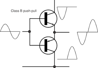
What about power amplifier? Aims to increase the power amplifier output signal power. In the course of this analog electronics, applied as a power amplifier on the speakers. At this power amplifier, the output voltage is set equal to the dc input voltage. While the current value of that changed. Does anyone know why the power amplifier, the voltage is fixed while the current is changed. I think changing the output flow is easier than changing the voltage output. And voltage range that can be applied is much smaller than the current range. Therefore it can be, the required current is very large so that in choosing a transistor must be adapted to current needs. If very large currents are needed at all, then it can be used Darlington transistor circuit. When I buy a transistor which has a large maximum collector current (about 1.5 A) appeared to form transistors is different from that so far I bought. At the center hole is used to heat sink. Heat sinks are used for fast component is not hot. By mounting the heat sink transistor then expand the surface so that heat more quickly thrown into the air. The price is relatively the same as a small power transistor. Btw, the actual power amplifier is a class B amplifier Class B amplifier is very efficient because the transistor will be active only when no signal input. Class B amplifier circuit consists of two identical transistors where each transistor is alternately brought in each half cycle. But there are drawbacks as well, the base emitter such as a diode that will be active when it has reached the forward bias voltage. So when the turn on off is not the same. Cause distortion of cross-over events. Form the output signal distortion due to cross-over is not expected that it needs considerable effort to overcome them. The solution is to arrange for the active transistor so that the need for constant base current (very small) even when it brought the transistor is not named as a class AB amplifier circuit.
Read More..