Showing posts with label using. Show all posts

Thursday, December 26, 2013

Latch Up Alarm Using Opto Coupler

The latch-up alarm described here is based on single IC NE555, configured as an astable multivibrator. The timing components are selected such that the oscillation frequency of the multivibrator lies within the audio range. Instead of a flip-flop stage, an opto-coupler (MCT2E) is used for latching of the alarm.  Under normal condition, pin 4 of IC1 is pulled to ground via resistor R2, and its output at pin 3 is held  ‘low’. When switch S1 is pressed momentarily, transistor T1 conducts to bring reset pin 4 of 555 to logic  ‘high’. As a result, IC1 is activated and the alarm starts to sound.
 
Latch-Up Alarm Using Opto-Coupler Circuit Diagram

Latch-Up Alarm Using Opto-Coupler Circuit-Diagram

 
Simultaneously, the LED inside opto-coupler glows and the phototransistor conducts. As a result, trigger transistor T1 gets base bias via phototransistor and resistor R6. The alarm sounds continuously until reset switch S2 is pressed. When switch S2 is pressed, transistor T1 is switched  ‘off’ to bring pin 4 of IC1 to logic ‘low’ and the alarm is disabled.


Source:   http://www.ecircuitslab.com/2012/01/latch-up-alarm-using-opto-coupler.html


Read More..

Saturday, December 21, 2013

Voltage Inverter Using Switch Mode Regulator

This circuit uses a step-up switch-mode regulator, which is usually used to produce a positive supply, to generate a regulated negative output voltage. The device used here is the MIC4680 from Micrel (www.micrel.com), but the idea would of course work with similar regulators from other manufacturers. Because of coil L1, which performs the voltage conversion by the intermediate storage of energy in the form of a magnetic field, the output is effectively isolated from the input. We can therefore connect the right-hand side of L1 to ground rather than to the positive output without causing a large current to flow. Then we connect the ground pin of the regulator IC and all the components connected to it as the negative voltage output, isolated from ground.

Voltage Inverter Using Switch-Mode Regulator

The components on the output side of the regulator are connected as usual: flywheel diode D1, coil L1 and the voltage divider formed by R1 and R2. These last two components set the output voltage, according to a formula given in the data sheet. Example component values for the MIC4680 used here are given in the table. The input voltage should lie within the permitted range for the regulator used, and must in any case be at least as great in magnitude as the desired output voltage (here +5 V or +12 V), so that the step-down regulation technique can wor.

Voltage Inverter Using Switch-Mode Regulator Table
It is important to take care when building this circuit to mount the regulator using an insulator, since generally the GND pin of the device is connected to the heatsink tab. Also, the ON/OFF control input cannot be driven using a normal logic signal, since the regulator’s ground reference is the output voltage rather than ground itself. If the ON/OFF function is required, a level shifter or optocoupler must be used.

Source: http://www.ecircuitslab.com/2011/06/voltage-inverter-using-switch-mode.html 
Read More..

Friday, December 20, 2013

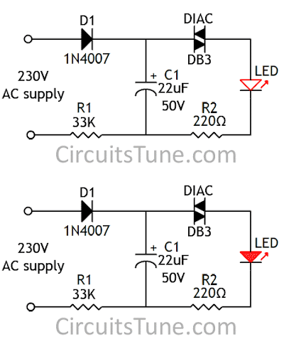
230V Led Flasher Circuit using DIAC

This is a very simple LED flasher circuit diagram that is powered from AC 230V mains. This Flasher can be used as a power indicator for the AC 230V mains supply. This circuit is made with few numbers of parts namely, a LED, two Resistors, one Capacitor, one Diode and one DIAC.  The DIAC act the main role to flashing the LED. DIAC is a bidirectional device. It conducts current only after its breakover voltage has been reached its threshold. Most DIACs break-over voltage is around 30 V.


230V Mains Power Indicator LED Flasher Circuit Diagram


230V Led Flasher
Fig: Circuit Diagram of 230V Led Flasher

When mains is connect to the circuit, the Capacitor(C1) starts charging through Diode(D1) and Resistor(R1). When the voltage on the capacitor reached the DIAC’s threshold voltage, the DIAC get turn on. And LED gets Lights(flash). At the same time Capacitor(C1) goes discharges and breakover voltage of DIAC also decrease and LED turns OFF. The on off time of the LED depends on the value of Capacitor(C1)  and Resistor(R1).
Note that the flashing time of the LED shown in the animating figure is not the exact timing of ON/OFF.
Read More..

Wednesday, October 9, 2013

Solar Lamp using the PR4403

The PR4403 is an enhanced cousin of the PR4402 40 mA LED driver. It has an extra input called LS which can be taken low to  turn the LED on. This makes it very easy  to build an automatic LED lamp using a  rechargeable battery and a solar module. The LS input is connected directly to the solar cell, which allows the module to be  used as a light sensor at the same time as  it charges the battery via a diode. When  darkness falls so does the voltage across  the solar module: when it is below a thresh-old value the PR4403 switches on. During  the day the battery is charged and, with  the LED off, the driver only draws 100 µA.
Circuit Diagram :
Solar Lamp-Circuit Diagram
At night the energy stored in the battery is released into the LED. In contrast to similar designs, here we can make do with a single  1.2 V cell. The PR4403 is available in an SO-8 pack-age with a lead pitch of 1.27 mm. The  other components are a 1N4148 diode (or a Schottky 1N5819) and a 4.7 µH choke. Pin 2 is the LS enable input, connected directly to the solar module. According to the datasheet, it is possible to connect a series resistor at this point (typ. 1.2 M) to increase the effective threshold voltage. The LED will then turn on slightly earlier in the evening before it is not completely  dark. Pins 3 and 6 of the device must be connected together and together form the output of the circuit.
Author : Burkhard Kainka - Copyright : Elektor
Read More..

Saturday, October 5, 2013

Boomer Audio Power Amplifier Using LM4906

The well-known LM386 is an excellent choice for many designs requiring a small audio power amplifier (1-watt) in a single chip. However, the LM386 requires quite a few external parts including some electrolytic capacitors, which unfortunately add volume and cost to the circuit. National Semiconductor recently introduced its Boomer® audio integrated circuits which were designed specifically to provide high quality audio while requiring a minimum amount of external components (in surface mount packaging only). The LM4906 is capable of delivering 1 watt of continuous average power to an 8-ohm load with less than 1% distortion (THD+N) from a +5 V power supply. The chip happily works with an external PSRR (Power Supply Rejection Ratio) bypass capacitor of just 1µF minimum.

In addition, no output coupling capacitors or bootstrap capacitors are required which makes the LM4906 ideally suited for cellphone and other low voltage portable applications. The LM4906 features a low-power consumption shutdown mode (the part is enabled by pulling the SD pin high). Additionally, an internal thermal shutdown protection mechanism is provided. The LM4906 also has an internal selectable gain of either 6 dB or 12 dB. A bridge amplifier design has a few distinct advantages over the single-ended configuration, as it provides differential drive to the load, thus doubling output swing for a specified supply voltage. Four times the output power is possible as compared to a single-ended amplifier under the same conditions (particularly when considering the low supply voltage of 5 to 6 volts).

LM4906 Boomer Audio Power Amplifier circuit schematic

When pushed for output power, the small SMD case has to be assisted in keeping a cool head. By adding copper foil, the thermal resistance of the application can be reduced from the free air value, resulting in higher PDMAX values without thermal shutdown protection circuitry being activated. Additional copper foil can be added to any of the leads connected to the LM4906. It is especially effective when connected to VDD, GND, and the output pins. A bridge configuration, such as the one used in LM4906, also creates a second advantage over single-ended amplifiers. Since the differential outputs, Vo1 and Vo2, are biased at half-supply, no net DC voltage exists across the load.

This eliminates the need for an output coupling capacitor which is required in a single supply, single-ended amplifier configuration. Large input capacitors are both expensive and space hungry for portable designs. Clearly, a certain sized capacitor is needed to couple in low frequencies without severe attenuation. But in many cases the speakers used in portable systems, whether internal or external, have little ability to reproduce signals below 100 Hz to 150 Hz. Thus, using a large input capacitor may not increase actual system performance. Also, by minimizing the capacitor size based on necessary low frequency response, turn-on pops can be minimized.
Read More..

Friday, October 4, 2013

Telephone Ringer Using Timer ICs

Using modulated rectangular waves of different time periods, the circuit presented here produces ringing tones similar to those produced by a telephone. The circuit requires four astable multivibrators for its working. Therefore two 556 ICs are used here. The IC 556 contains two timers (similar to 555 ICs) in a single package. One can also assemble this circuit using four separate 555 ICs. The first multivibrator produces a rectangular waveform with 1-second ‘low’ duration and 2-second ‘high’ duration. This waveform is used to control the next multivibrator that produces another rectangular waveform. A resistor R7 is used at the collector of transistor T2 to prevent capacitor C3 from fully discharging when transistor T2 is conducting. Preset VR1 must be set at such a value that two ringing tones are heard in the loudspeaker in one second.

Telephone Ringer Using Timer ICs circuit diagram
The remaining two multivibrators are used to produce ringing tones corresponding to the ringing pulses produced by the preceding multivibrator stages. When switch S1 is closed, transistor T1 cuts off and thus the first multivibrator starts generating pulses. If this switch is placed in the power supply path, one has to wait for a longer time for the ringing to start after the switch is closed. The circuit used also has a provision for applying a drive voltage to the circuit to start the ringing. Note that the circuit is not meant for connection to the telephone lines. Using appropriate drive circuitry at the input (across switch S1) one can use this circuit with intercoms, etc. Since ringing pulses are generated within the circuit, only a constant voltage is to be sent to the called party for ringing.

Note.
  • To resemble the actual telephone ringing a 400 Hz tone is switched on in the following sequence: 400ms on, 200ms off, 400ms on and 2000ms off and then repeat.
Read More..

Tuesday, October 1, 2013

How To Connect Two Computers Using Modems

Have you ever connected two PCs together via modems using a twisted pair cable and nothing happened? That’s because the modems are expecting a phone line with all the signals and voltages supplied by the local telephone exchange. This circuit simulates the DC power and signal isolation but not the "dial tone" or the "ring signal". It suffices to connect two PCs together to communicate and exchange files using HyperTerminal.
The circuit is self-explanatory and needs only one power supply for both modem lines. Although 50V DC is the usual exchange line voltage, this circuit should operate down to 20V. A 600O line transformer (eg. Jaycar cat. MM-1900) provides signal isolation, while the resistors provide current limiting and keep the lines as balanced as possible. When using this set-up with HyperTerminal, you should not select a Windows modem driver in the "Connect To" dialog. Instead, connect directly to the relevant COM port.
connect-two-pcs-using-modems

Next, verify that the modems are working by sending information commands such as "ATI1" or "ATI3". If you don’t get a response using these commands, try resetting the modem(s) using the "AT&Z" command. Assuming you do get a response, set one in originate mode using the "ATD" command and the other in answer mode with the "ATA" command. If all is well, you should now be able to type in one terminal window and see the results echoed in the second PC’s terminal window. To return to control mode, type "+++". The advantage of using modems instead of a serial cable between COM ports is that the two PCs can be kilometres apart instead of a few metres. For example, you could connect the house PC to the workshop PC on the other side of the farm.
Author: Filippo Quartararo - Copyright: Silicon Chip Electronics
Read More..

Sunday, September 22, 2013

Fan Controller Using Just Two Components

The Maxim MAX 6665 (www.maxim-ic.com) provides a complete temperature-dependent fan controller. It can switch fans operating at voltages of up to 24 V and currents of up to 250 mA. The IC is available from the manufacturer in versions with preset threshold temperatures between +40 °C (MAX6665 ASA40) and +70 °C (MAX6665 ASA 70). The device’s hysteresis can be set by the user via the HYST input, which can be connected to +3.3 V, connected to ground, or left open. The following table shows the hysteresis values available:

HYST = Hysteresis
open = 1 °C
ground = 4 °C
+3.3V = 8 °C
Fan Controller Circuit DiagramThe other pins of the SO8 package are the FORCEON input and the status outputs WARN, OT and FANON. The test input FORCEON allows the fan to be run even below the threshold temperature. The open-drain output WARN goes low when the temperature rises more than 15 °C above the threshold temperature, while the open-drain output OT indicates when the temperature is more than 30 °C above the threshold. The push-pull output FANON can be used to indicate to a connected microcontroller that the fan is turned on.
Read More..

Saturday, September 21, 2013

Battery Charger Display Using LT1639

The Over-the-Top type of operational amplifier is ideal for use as a current sense for battery charger applications. The design described here can be used with chargers for rechargeable batteries (Lead/acid or NiCd etc). The 5 V operating supply for the circuit is derived from the battery on charge. The circuit uses a sense resistor R8 to determine the value of current flowing in or out of the battery. An LED output shows whether the battery is charging or discharging and an analogue output displays the battery charge or discharge current. The circuit can also be altered to shown different ranges of charging current to cater for higher capacity cells. IC1a and IC1b together with T1 and T2 form two current sources, which produce a voltage across R5. The voltage across R5 is proportional to the current through resistors R8 and R1 (for IC1a) or R8-R3 (for IC1b).

Battery Charging indicator circuit diagramThe current source formed by IC1a and T1 is active when the batteries are discharging and IC1b and T2 is active when the batteries are being charged. In each case the inactive opamp will have 0V at its output and the corresponding transistor will be switched off. IC1d amplifies the voltage across R5, which is proportional to the sense current. The component values given in the diagram produce an amplification factor or 10. A sense current of 0.1 A will produce an output voltage of +1 V. The supply voltage to the circuit is +5 V so this will be the maximum value that the output can achieve. This corresponds to a maximum charge/discharge current of 0.5 A To display currents from 0 to 5.0 A, resistor R7 can be omitted to give IC1d a voltage gain of 1.

Higher currents can be displayed by using a lower value of sense resistor R8. A DVM or analogue meter can be used at Vout to give a display of the charge/discharge current. The constant current sources can only function correctly when the supply to the voltage regulator circuit (UBatt. e.g. 6V or 12V) is greater than the operating voltage of the opamps (+5 V). The supply voltage to the LT1639 can be in the range of +3 V and +44V and voltages up to 40V over the supply voltage are acceptable at the inputs to the opamp. IC1c controls the charging/discharging LED output. The inputs to this opamp are connected to the outputs of the current source opamps and its output goes high when the battery is being charged and low when it is discharging.
Read More..

Thursday, September 5, 2013

Audio Amplifier Using TDA1519

This audio amplifier circuit is based on the TDA1519 amplifier ic which can be used in audio applications which don’t need high output power .The TDA1519 circuit can deliver 2x6 watts output power .

Audio Amplifier Circuit Using TDA1519

TDA1519 is an integrated class-B dual output amplifier in a 9-lead single in-line (SIL) plastic medium power package is primarily developed for car radio applications.This amplifier electronic circuit project needs to be powered from a 14.4 volt DC power supply
Read More..

Sunday, May 19, 2013

Measuring motor insulation using HI POT tester

What is HI-POT tester?
When we need to evaluate motor condition,HI-POT tester or High Potential tester is the common equipment are used.As we know,a multimeter or ohm meter reading only can determine if a motor winding is open or shorted but cannot checked winding insulation condition if shorted with ground or phase.
The main purpose of the Hi Pot tester is to verify the quality and integrity of the electric motor insulation materials used on the armature or stator and also safe to using it without any defect.
Sometime we not take a serious attention or not know about it to checked winding insulation.This step is important to ensure motor can running in good condition without any breakdown.
Normally electrical motor may have a weakened winding that shorts to ground when it running.It have several caused for the winding breakdown due to the value of system voltage,winding heat build up or overloaded mechanical stress.For other caused it will come from motor terminal board that has an insulation failure from the terminal to ground (earth) or from other terminal for winding connection.

Basic operation of HI-POT Tester
A HI-POT tester produce power source with a high voltage (Volt) and low current (ampere) and it is used to check for an insulation failure for motor winding that the ohmmeter cannot measure with its low voltage power source may miss.
It measures winding insulation resistance to ground (earthing) and terminal board resistance from terminal to ground and from terminal to terminal ( phase to phase )
To get a best result and for safety reason when perform measurement for winding insulation resistance,all wiring is removed from the motor winding terminals.It also same when perform measurement for terminal board resistance, all wiring is removed from the terminal board.
Below is several rules when using the Hi-Pot tester.It is to avoid any serious damage or injuries during insulation measurement and should never be :

1. Operated alone or by an inexperienced service person.
2. Set at a voltage of more than twice the motor operating voltage plus 1000 volts.
3. Be set for more than 5 milliamps without consulting or refer user manual from motor manufacture
4. Applied for more than the time it takes to obtain a reading (no more than a few seconds).
5. Used as a phase-to-phase winding check.
6. For air condition motor compressor,used when the system is in a vacuum.

* SAFETY NOTE : Please read HI-POT tester user manual before using it and refer to the trained or qualified person for assist during measurement.It the best way to avoid any unexpected issued and for safety reason.
Read More..

Friday, April 12, 2013

50 W Power Amplifier Circuit using STK084

50W Power Amplifier Circuit using STK084

This is the circuit diagram of 50W power amplifier circuit which built based on single power amplifier chip of STK084. Its an well-known old IC for audio frequency (AF) amplifier.

This circuit requires dual polarity / split power supply with maximum supply of ± 50. The recommended supply is ± 35 / 2-3A DC current. You may use this split power supply circuit for the amplifier. Use 28V center tap transformer to get about ± 36V output.

Technical Details:
Power output: 50W
RL : 8 Ohm
TDH : 0.2 %
Rin : 52K
Gain : 26.4 dB
Noise : 0.3 mV

Take a note that heatsink is required to be mounted on the power IC since it will going to hot when operated and deliver high power output (high audio volume level). Link
50W Power Amplifier Circuit using STK084,
Read More..

Thursday, April 11, 2013

70W POWER AMPLIFIER USING 2N30055 MJE2955 CIRCUIT DIAGRAM

70W POWER AMPLIFIER USING 2N30055 - MJE2955 CIRCUIT DIAGRAM

This amplifier is fairly well behaved for turn on, and should issue (at worst) the smallest click as power is applied. When power is removed, after about 5 seconds or so, there will normally be a low level thump - this is not dangerous to speakers, unless used in tri-amp and directly connected to the tweeters - DO NOT DO THIS - not with any amp. Always use a capacitor in series with tweeters (see Bi-Amplification, Some thoughts on Tri-Amping).
Read More..

Monday, April 8, 2013

Digital Stop Watch Using NE555 Timer IC

This is s design of digital stop watch circuit that built around timer IC LM555 and 4-digit counter IC MM74C926 with multiplexed 7-segment LED display. This is the figure of the circuit.


MM74C926 consists of a 4-digit counter, an internal output latch, NPN output sourcing drivers for common cathode, 7-segment display and an internal multiplexing circuitry with four multiplexing outputs. The counter advances on negative edge of the clock. The clock is generated by timer IC LM555. The circuit works off a 5V power supply. It can be easily assembled on a general-purpose PCB. Enclose the circuit in a metal box with provisions for four 7-segment displays, rotary switch S1, start/stop switch S2 and reset switch S3.

For operation this circuit is explanation in the next. First, reset the circuit by pressing S3 so that the display shows ‘0000.’ Now open switch S2 for the stop watch to start counting the time. If you want to stop the clock, close S2. Rotary switch S1 is used to select the different time periods at the output of the unstable multi vibrator (IC1). This circuit is powered by 5V DC. That power supply can take from regulator power supply. You can read in this site about the regulator that can be used.

Read More..

Thursday, April 4, 2013

Inverter Circuit Using IC 4069 Discussed

Please read the previous post for the continuation...

Hi Aliman,
I am interested to follow the output stage exactly as given in your square wave design. I want you to include all the MOSFETs - NP as well as PN along with the buffer transistors and their base resistors.


The logic is very simple, if the output stage is responding and working well with the signals from the IC 4069, it should do the same with the signals from the 4017 ICs, after all both the designs are producing square waves (our design is producing a chopped one though.)

The voltages that you are getting are absolutely fine and the differences are too trivial to produce any effect on the circuit, moreover, very unlike the transistors, for MOSFETs its the voltage that matters and not the current and thats why the buffer transistors become very important and must be included.


I think it will be also important to include 10K resistors from the base of each buffer transistor to GROUND.

I wont be able to help you with the MOSFET types, as I myself am not quite knowledgeable with these devices, but the above modifications should hopefully set things in the right order.

Thanks and Best Regards.

Hi Swagatam, what if I replace the buffer transistor with one that has a higher collector current. Would that make a difference ?
 Also you mentioned adding 10K resistors, because there already is a 10K resistor from the 4069 to the base of the buffer transistor, so you want me to add another 10K from the Base to ground ,  correct ?
I dont have any PNP mosfets right now. But if this output stage works with the Square wave circuit , with some minor changes our PWM circuit should work also.
Sincerely Ali 

Hi Aliman,

I think we better stick to the tested design given below, so lets follow the circuit as given in your square wave design... we can always modify it once it starts working.

Thats correct... The 10K resistor from the base of the transistors to the ground will ensure that every time the diodes stop conducting the base receives a ground or a low logic level and switches OFF completely.

Yes..of-course, if it starts working then the issue gets over and we wont need to include the PNPs.

Best Regards.


Continued HERE,
Read More..

Tuesday, April 2, 2013

Battery Charger Circuit Using Ammeter VU

This is a design of the circuit diagram of a simple and straight forward battery charger that can be used to charge all type of 12V rechargeable batteries including car batteries. This circuit is completed with ammeter VU for displaying the current. This is the figure of the circuit.


The circuit is nothing but a 12V DC power supply with an ammeter for monitoring the charging current. The two diodes forms a centre tapped full wave rectifier. The capacitor filters the rectifier output to produce a clean 12V out put. At initial stages of charging the ammeter will read about 1 to 3 amperes. As the battery is slowly charged the current slowly decreases. For indicate when the battery is fully charged, the ammeter reading will be zero. For attention, it is always be careful to connect the charger to the battery in correct polarity. The polarity is connecting between positive to positive and negative to negative.

Read More..